In this part we are going to focus on more features of STM8 (clock, EEPROM, option bytes, flash access) and stick some wires into the mains outlet.
Contents:
Clock
STM8 can run on one of 3 different clock sources:
- External clock/crystal oscillator (HSE)
- Internal 16 MHz RC oscillator (HSI)
- Internal 128 khz RC oscillator (LSI)
These clock sources determine the frequency of master clock which clocks the CPU and peripherals. HSI clock can be scaled down by adjusting 2-bit HSIDIV prescaler. At startup the master clock source is automatically selected as HSI / 8, which results in 2 MHz. It is possible to decrease CPU frequency by increasing the prescaler value in CPUDIV register. By default the prescaler is set to 1.
In the previous part we didn’t bother configuring clocks and therefore were running at 2 MHz. This time we’ll be using an external crystal connected between PA1 and PA2 pins. Before we start configuring clocks, let’s take advantage of processor’s clock output capability - this will allow us to perform a sanity check and see if we configured things properly.
1 |
|
Various clock output options are available in the CLK_CCOR register - I defined some of the possible ones so that you get the idea.
Enabling external oscillator is done by setting HSEEN bit in CLK_ECKR register. As soon as the oscillator is ready (which is indicated by HSERDY bit), we need to switch the master clock to HSE by writing 0xB4 into CLK_SWR. Finally, we wait until the clock source is stabilized and execute the clock switch by setting SWEN bit in CLK_SWCR.
1 | void hse_enable() { |
External clock
There is a nice trick when you need to sync two or more microcontrollers: instead of using a crystal you can supply an external clock to the oscillator input pin and leave the other pin floating. STM8 even has a dedicated mode for external clock source, which can be activated by enabling EXTCLK option bit.
The procedure for enabling external clock is identical to enabling HSE, except that we don’t write HSEEN bit, since we’re not driving an oscillator. In this case I used automatic clock switching mechanism: the only difference is that it allows the processor to run and execute instructions while the clock is being stabilized, although I’m still polling for SWIF since I want to stall the CPU until the clock switching is complete.
1 | void external_clock_enable() { |
After connecting the external clock source to OSCIN (PA1), we need to enable EXTCLK option bit by writing 0x08 into OPT4 (option bytes will be discussed later on). Finally, we call external_clock_enable() and wait until the CPU switches clocks. We can ensure that clock switching is successful by enabling clock output and probing CLK_CCO pin.
The external clock source has to be a square wave with 50% duty cycle. According to the documentation, sine and triangle waveforms can be used as clock sources as well. The datasheet also claims that minimum CPU frequency is 0 Hz.
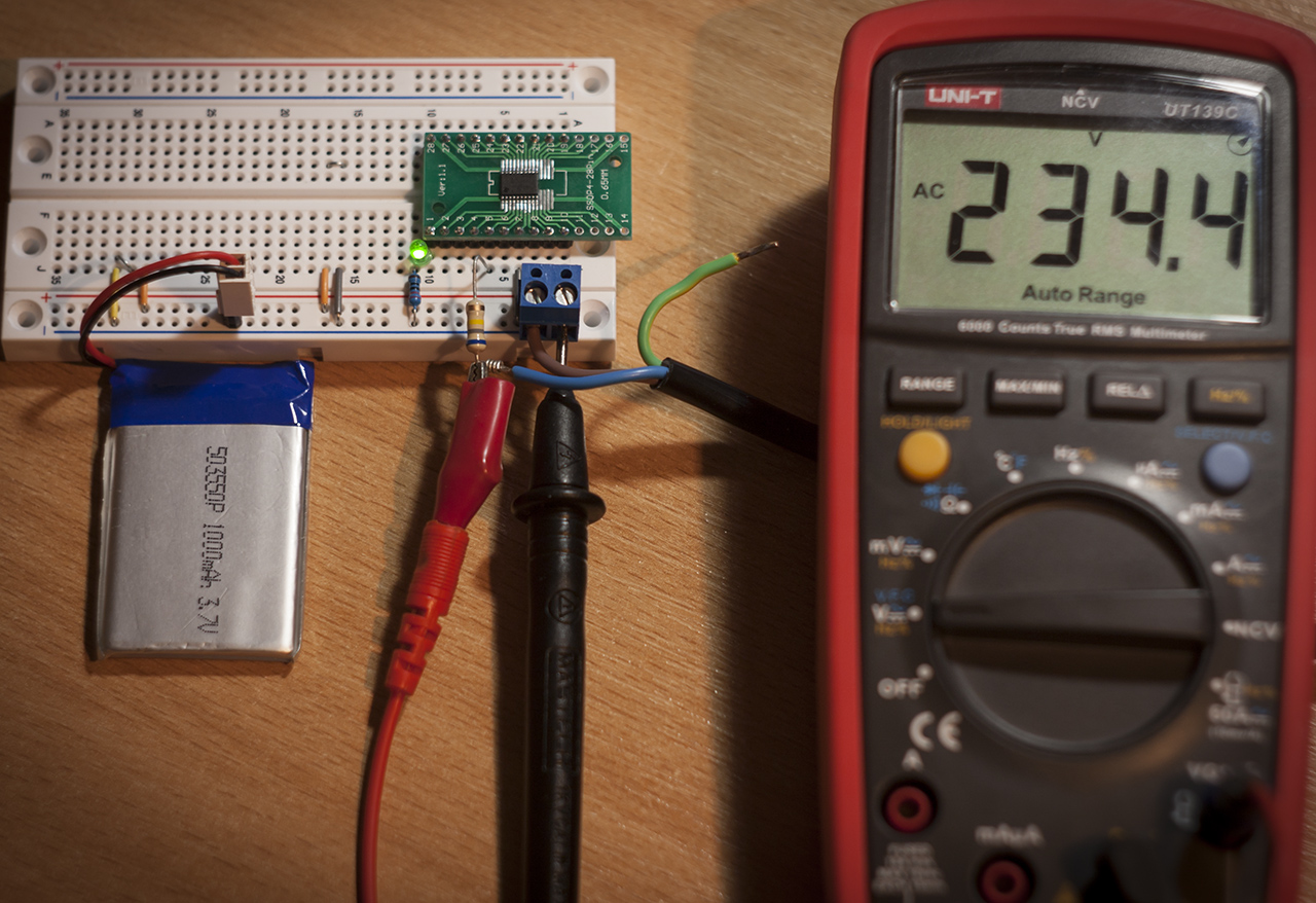
So, presumably, it’s possible to clock the CPU from a sinusoidal signal with frequency all the way down to DC. Ugh.. the temptation is irresistible. I don’t have a signal generator. But I do have mains AC.

Surprisingly, it worked. In case you’re wondering, the chip was able to survive 230V applied to it due to the fact that every pin on STM8 (except for ‘true open-drain’ pins) has protection diodes to Vcc and ground. These diodes will clamp any excessive voltages and prevent the part from releasing the magic smoke. Having a large value series resistor limits the current flowing through these diodes. The documentation doesn’t specify maximum current for clamping diodes, but it’s usually a good idea to keep it below 1mA. Keep in mind that when the diodes conduct the current has to return somewhere - in this case it’s the lithium battery. Did I mention that it’s not a particularly good idea?
A less lethal approach
Although clocking the MCU directly from mains was kind of fun, I felt rather uncomfortable working when the microcontroller is live. Since I still wanted to find out how useful a mains-clocked processor is, I decided to make things a bit less hazardous by adding some opto-isolation.
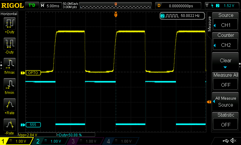
I discovered that the clock input circuitry does not like low frequency signals with slow edges. Feeding the output of the opto-isolator directly into the microcontroller results in random glitches on the clock output due to false triggering, and occasionally the CPU just locks up. Applying mains directly worked better since the slew rate was higher in that case. The datasheet hints that HSE has to be above 1 MHz for external crystal, but doesn’t specify the lower limit for external user clock. I’m pretty sure we can get stable operation if we improve transition speed. For this purpose we’ll need to use a Schmitt trigger, which is basically a comparator with hysteresis, to convert the output of the optocoupler into a nice and clean square wave.
There are dedicated Schmitt trigger ICs and even opto-isolators with Schmitt trigger outputs - non of these do I have at hand. One can implement a Schmitt trigger using an op-amp, but if you want to save a few resistors you can use a good old 555 timer. The 555 has two comparators configured to fire off when voltage on their inputs reaches 1/3 and 2/3 Vcc respectively, which is just about right to set the hysteresis. Comparator inputs are pins 2 (Trigger) and 6 (Threshold). Below is the resulting schematic.

R1 is limiting the current flowing through the LED inside the optocoupler and D1 guarantees that reverse breakdown voltage of the LED would not be exceeded during the negative half cycle of the sine wave. Resistor values depend on the optocoupler being used. In my case I used LTV-817 (Vf = 1.2V) and R1 will limit the peak current to Ipeak = (325 - 1.2) / 180000 = 1.8mA. Since the threshold is fixed, I had to adjust R2 to get as close to 50% duty cycle as possible, which is why it’s value ended up being higher than it should be.
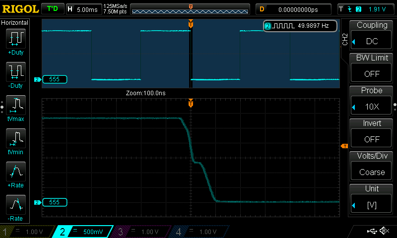
The only timer that I had was NE555 - it’s quite a slow chip not rated for 3.3V operation. A CMOS timer like LMC555 would be a much better choice. That being said, the resulting waveform is still acceptable.

The duty cycle isn’t precisely 50% and the edges are a bit jagged and jittery, but still good enough for the processor to latch onto.

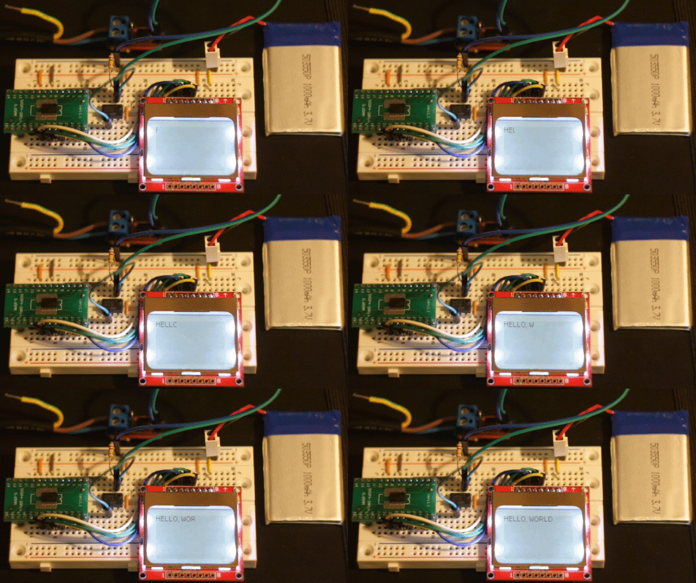
After connecting the output of the Schmitt trigger to OSCIN, I ensured that I was getting a stable 50 Hz output on CLK_CCO pin and tried bringing up various peripherals. Below is the sped up footage of one of my experiments.

Well, that was the slowest SPI communication I’ve ever seen. Nevertheless, it was nice to know that the processor is still usable at such low clock frequencies.
EEPROM
EEPROM is a small area of memory that can be used for storing things like configuration, calibration data, etc. On STM8S003 EEPROM starts at address 0x4000 and ends at 0x407F, which results in stunning 128 bytes of data. Let’s define some macros first. We’ll use the first macro for memory access, just like we did with register definitions in part 1.
1 |
By default, EEPROM is write protected and a specific sequence is required in order to unlock it: two hardware keys have to be written into FLASH_DUKR register. The first time I tried programming EEPROM it didn’t work. The reason was me ignoring the following statement in the reference manual: “before starting programming, the application must verify that the DATA area is not write protected”. I interpreted it as “you shouldn’t write into write-protected areas” while the real meaning was “it takes some time to unlock EEPROM”.
1 | void eeprom_write(uint16_t addr, uint8_t *buf, uint16_t len) { |
Note that on low density STM8S microcontrollers the CPU is stalled during EEPROM write operation, therefore it is not necessary to poll for EOP flag.
Reading EEPROM is achieved the same way you read any other memory:
1 | void eeprom_read(uint16_t addr, uint8_t *buf, int len) { |
Interestingly, flash programming manual states that on low density devices, EEPROM is comprised of additional 640 bytes of memory located in the same memory array with flash. In other words, it seems like there are 10 pages of flash memory reserved for EEPROM. Also, the manual gives the exact value (it doesn’t say up to 640 bytes), which contradicts with the datasheet.
Let’s try shifting EEPROM_END_ADDR to 0x4280 and filling the whole range with dummy bytes:
1 | void main() { |
Now we can dump EEPROM and check if it was written. I deliberately specified stm8s103f3 to read more memory than our part has.
1 | stm8flash -c stlinkv2 -p stm8s103f3 -s eeprom -r dump.bin |
Yeap, it worked on every processor that I tried. Although I would rather prefer having a bit more flash memory, it’s still good to know that STM8S003 has some extra EEPROM.
Option bytes
Option bytes are located in the EEPROM and allow configuring device hardware features such as readout protection and alternate function mapping. Each option byte, except for read-out protection, has to be stored in a normal form (OPTx) and complementary form (NOPTx). The procedure for writing option bytes is the same as for writing EEPROM, except for the unlcok sequence: OPT bit has to be set in FLASH_CR2 and FLASH_NCR2 registers.
1 | void opt_write() { |
If you mess things up, you can reset the option bytes via SWIM:
1 | $ echo -ne '\x00\x00\xff\x00\xff\x00\xff\x00\xff\x00\xff' > opt.bin |
Interestingly, if we read the memory a bit further, we find a section which contains the following data:
1 | 0x480B: 00 00 00 00 00 00 00 00 00 00 00 00 00 00 00 00 00 00 00 00 00 00 00 00 |
20 bytes at address 0x4840 are written with their complement values just like the option bytes. This whole block is write protected and differs slightly from one processor to another - unique ID perhaps?
Flash
One thing that I like the most about STM8 is flash access.
The two most common types of flash memory are NAND and NOR flash. Flash is physically divided into blocks, which may be further divided into sectors. The entire memory is linear and can be read or written in a random access fashion, however both NAND and NOR flash share the same disadvantage: you can flip a 1 into a 0 but not vice-versa. The only way to flip a 0 back to 1 is to erase the whole block. If you need to overwrite a few bytes in flash memory you have to buffer the whole page into RAM, modify the buffer, erase flash page and write the buffer back into flash memory - the whole process is rather time-consuming.
With STM8 this is not the case: the whole memory can be accessed at byte level. You can write any byte inside any page and erase it by simply writing 0x00 at that address. Essentially, you can treat flash memory as a large EEPROM.
Removing write protection is almost identical to unprotecting EEPROM.
1 | void flash_write(uint16_t addr, uint8_t *buf, uint16_t len) { |
Just like with EEPROM, we can dump the entire flash memory:
1 | stm8flash -c stlinkv2 -p stm8s003f3 -s flash -r dump.bin |
SDCC has various attributes like __xdata and __eeprom for placing things in specific memory locations. Unfortunately, none of them are implemented for STM8 yet. We can partially work around this limitation by using __at attribute:
1 | /* Use last 64 bytes of flash for user data */ |
Let’s take a closer look at the above example: first we define two addresses in flash memory. Remember that program memory starts at 0x8000, so we add this value to get the address we want. Next we declare data array with attribute __at(USER_DATA_ADDR) - this tells the compiler where to look when the variable is being accessed. For example, a read operation on data[2] will return the value at address 0x9FC3, which is the same as calling _MEM_(0x9FC3). Same goes for write operation: if flash is unlocked, then writing data[2] will store the value at the appropriate address in flash memory. If flash unlock sequence was not executed before performing a write, then WR_PG_DIS bit will be set in FLASH_IAPSR register to indicate an attempt to modify write-protected page.
The second variable id is declared as const - this will actually produce a binary with the value placed at specified memory address. Declaring a variable as constant means that compiler will not allow us to perform explicit write operations, unless we write directly at the specified address (which kind of defeats the purpose of const qualifier). Unfortunately, this approach will not work for EEPROM - SDCC will simply produce a larger binary image.
That’s it for now. In the next part we’re going to take a look at some of the features essential for real-world applications and discuss questions of reliability and performance. As always, code is available on github. Since previous article the repository evolved into a small peripheral library with dedicated examples directory.